Circuit Diagram 3 Bit Parity Generator - Jika kamu mencari artikel Circuit Diagram 3 Bit Parity Generator terbaru, berarti kamu sudah berada di web yang tepat. Setiap artikel dibahas secara lengkap dengan penyajian bahasa yang gampang dipahami bagi orang awam sekalipun. itulah sebabnya situs ini banyak diminati para blogger dan pembaca online. Yuk langsung aja kita simak penjelasan Circuit Diagram 3 Bit Parity Generator berikut ini.
Circuit Diagram 3 Bit Parity Generator. 328 Derive the circuits for a three-bit parity generator and four-bit parity checker using odd parity bit. It is all completely free-----. Only 8 NAND gates would be needed. The table shows the parity generator outputs for various 4-bit data words. Exclusive OR operation of parity bit is a scheme for finding errors throughout transmission of binary information.
1978 Vw Bus Engine Diagram Now let us implement an even parity checker circuit. Somewhere I have a feeling that something was lost in translation and the actual question was some time ago How to draw a circuit diagram to check a 4 bits number is odd or even parity. Design and simulate the Parity. The given below circuit will provide the 4 bit parity checker circuit. 4-Bit Even Parity GeneratorContribute. State Machine diagram for the same Parity Generator has been shown below.
Derive the Boolean function for P c.
Open Circuit Detection Wiring Diagram 1 Youtube Now let us implement an even parity checker circuit. Consider input I is a stream of binary bits. Click here to realize how we reach to the following state transition diagram. The 9 bit 8 data bits 1 parity bit Parity GeneratorChecker is shown in the below figure. State Machine diagram for the same Parity Generator has been shown below. If even then the output becomes 0 O 0 otherwise output would be 1 O 1.
4-Bit Even Parity GeneratorContribute.
8051 Pin Diagram Wikipedia Consider input I is a stream of binary bits. Somewhere I have a feeling that something was lost in translation and the actual question was some time ago How to draw a circuit diagram to check a 4 bits number is odd or even parity. The circuit diagram of odd parity generator is shown in the following figure. Use a Truth Table to construct odd parity generator. The above circuit diagram contains two 2-input OR gates one 4-input OR gate one 2input AND gate an inverter.
Logic diagram of 4-bit odd parity checker using EX-NOR gates.
Citroen C3 2002 Wiring Diagram The given below circuit will provide the 4 bit parity checker circuit. Derive the Boolean function for P c. Design a parity checker circuit for a 4-bit data. So the resultant word data contains 4 bits which will be received as the input of even parity checker. Now the output odd parity bit would be decided on the basis of 4 input bits namely A B C and D. Consider input I is a stream of binary bits.
Derive the logic circuit from algebraic function obtained from Truth Table.
1998 Buick Regal Starter Wiring Diagram IC 74180 Block diagram of parity generator and parity checker IC. As its name implies the operation of an Odd Parity generator is similar but it provides odd parity. 4 for AB and 4 for the output of the previous and C. Parity checker networks are logic circuits along with exclusive OR functions. If even then the output becomes 0 O 0 otherwise output would be 1 O 1.
The total number of 1s must be even to generate the even parity bit P.
2003 Ford F 250 Interior Lights Wiring Diagram As its name implies the operation of an Odd Parity generator is similar but it provides odd parity. Derive the logic circuit from algebraic function obtained from Truth Table. Design a logic circuit for a 3-bit message to be transmitted with an even parity bit. A circuit diagram for a 3 bit parity generator with only NAND gates used. Now the output odd parity bit would be decided on the basis of 4 input bits namely A B C and D. Lets design the Mealy state machine for the Even Parity Generator.
Somewhere I have a feeling that something was lost in translation and the actual question was some time ago How to draw a circuit diagram to check a 4 bits number is odd or even parity.
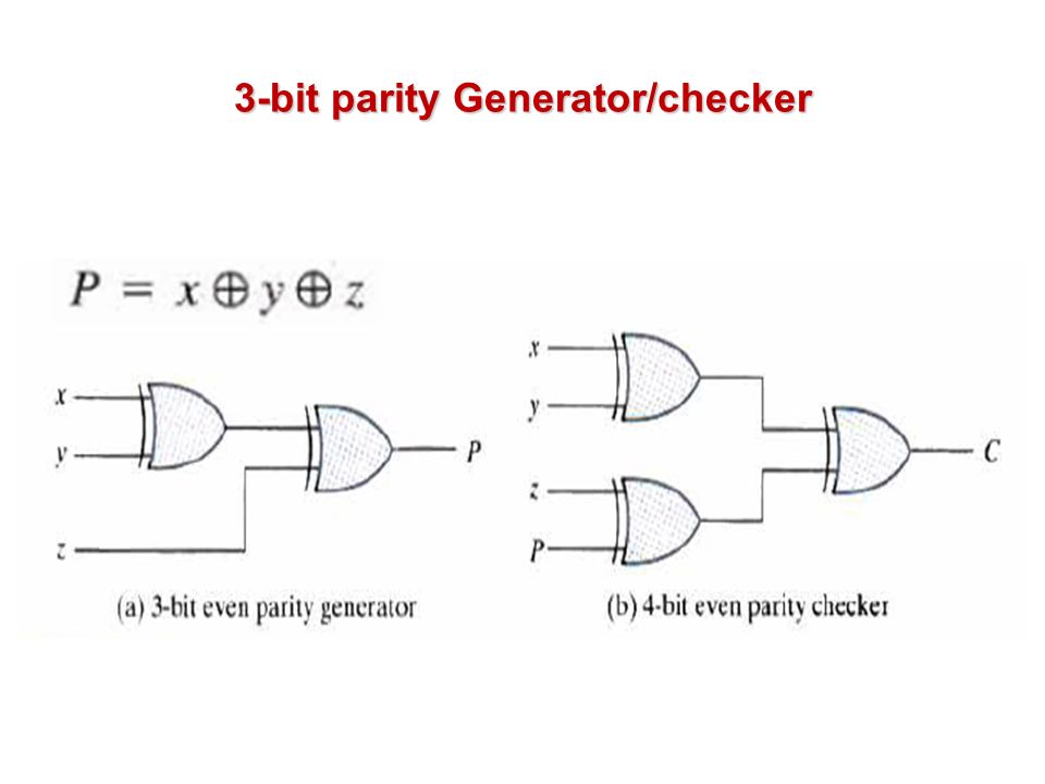
Fiat X19 Haynes Wiring Diagram Obtain the truth table for 3-bit odd parity generator function P b. Design a logic circuit for a 3-bit message to be transmitted with an even parity bit. The parity generator circuit will take 3 input bits x y and z and produce 1 output bit P. Design a parity checker circuit for a 4-bit data. If even then the output becomes 0 O 0 otherwise output would be 1 O 1.
The receiver calculates the parity bit of the.
In Out Wiring Diagram Fan In place of 3 input bits in the message signal if we have 4 bits then it becomes a 4-bit odd parity generator. 4 Bit Odd Parity Generator. Design and build a 3-bit odd parity generator. Somewhere I have a feeling that something was lost in translation and the actual question was some time ago How to draw a circuit diagram to check a 4 bits number is odd or even parity. Lets design the Mealy state machine for the Even Parity Generator. Design and build a 3-bit odd parity generator.
It is all completely free-----.
Programming And Meta Programming In Scheme Derive the logic circuit from algebraic function obtained from Truth Table. Design an evenodd parity generator for 4-bit data. A circuit diagram for a 3 bit parity generator with only NAND gates used. If even then the output becomes 0 O 0 otherwise output would be 1 O 1. The parity generator circuit will take 3 input bits x y and z and produce 1 output bit P.
This question is like how do I draw the circuit of a battery or a wire.
91 Buick Century Wiring Diagram As its name implies the operation of an Odd Parity generator is similar but it provides odd parity. 328 Derive the circuits for a three-bit parity generator and four-bit parity checker using odd parity bit. The above circuit diagram contains two 2-input OR gates one 4-input OR gate one 2input AND gate an inverter. Ic-74180 The IC 74180 contains eight data bits X 0 to X 7 V cc even input odd input Seven output S odd output and ground pin. Let the three inputs A B and C are applied to the circuits and output bit is the parity bit P. A parity bit is an extra bit included with a binary message to make the number of ls either odd or even.
The given below circuit will provide the 4 bit parity checker circuit.
1996 Honda Passport Stereo Wiring Diagram Consider input I is a stream of binary bits. Parity checker networks are logic circuits along with exclusive OR functions. 3-bit Odd Parity Generator circuit. Logic diagram of 4-bit odd parity checker using EX-NOR gates. Design and build a 3-bit odd parity generator.
6 329 Implement the following four Boolean expressions with three half adders.
2003 Chevrolet Suburban Wiring Diagram 31 Obtain the truth table for 3-bit odd parity generator function P P X y z 000 00 1 010 011 100 101 1 10 111 Derive the Boolean function for P using XOR gates only Draw the logic diagram and build the circuit using a single7486 chip. As its name implies the operation of an Odd Parity generator is similar but it provides odd parity. State Machine diagram for the same Parity Generator has been shown below. The table shows the parity generator outputs for various 4-bit data words. This question is like how do I draw the circuit of a battery or a wire. In place of 3 input bits in the message signal if we have 4 bits then it becomes a 4-bit odd parity generator.
Lets design the Mealy state machine for the Even Parity Generator.
2001 F250 7 3 Wiring Diagram Ef Circuit A parity bit is an extra bit included with a binary message to make the number of ls either odd or even. State Machine diagram for the same Parity Generator has been shown below. A parity bit is an extra bit included with a binary message to make the number of ls either odd or even. The parity generator circuit will take 3 input bits x y and z and produce 1 output bit P. The table shows the parity generator outputs for various 4-bit data words.
Now let us implement an even parity checker circuit.
2005 Ford Focus Wiring Diagram Original Derive the Boolean function for P c. Design an evenodd parity generator for 4-bit data. Design and build a 3-bit odd parity generator. 31 Obtain the truth table for 3-bit odd parity generator function P P X y z 000 00 1 010 011 100 101 1 10 111 Derive the Boolean function for P using XOR gates only Draw the logic diagram and build the circuit using a single7486 chip. 4 Bit Odd Parity Generator. Ic-74180 The IC 74180 contains eight data bits X 0 to X 7 V cc even input odd input Seven output S odd output and ground pin.
Surely the depth to which a question can be regarded as trivial has hit a new low.
Co Headlight Wiring Diagram So the resultant word data contains 4 bits which will be received as the input of even parity checker. Only 8 NAND gates would be needed. The receiver calculates the parity bit of the. Somewhere I have a feeling that something was lost in translation and the actual question was some time ago How to draw a circuit diagram to check a 4 bits number is odd or even parity. This question is like how do I draw the circuit of a battery or a wire.
Consider input I is a stream of binary bits.
1998 Ford F150 Stereo Wiring Diagram Design and build a 3-bit odd parity generator. The above circuit diagram contains two 2-input OR gates one 4-input OR gate one 2input AND gate an inverter. Draw the logic diagram and build the circuit using a single7486 chip. Design an evenodd parity generator for 4-bit data. Now the output odd parity bit would be decided on the basis of 4 input bits namely A B C and D. 4 for AB and 4 for the output of the previous and C.
Lets design the Mealy state machine for the Even Parity Generator.
Western 3 Port Isolation Module Wiring Diagram Use a Truth Table to construct odd parity generator. Here AND gate inverter combination are used for producing a valid code at the outputs even when multiple inputs are equal to 1 at the same time. 4 for AB and 4 for the output of the previous and C. Design and build a 3-bit odd parity generator. So the resultant word data contains 4 bits which will be received as the input of even parity checker.
Situs ini adalah komunitas terbuka bagi pengguna untuk membagikan apa yang mereka cari di internet, semua konten atau gambar di situs web ini hanya untuk penggunaan pribadi, sangat dilarang untuk menggunakan artikel ini untuk tujuan komersial, jika Anda adalah penulisnya dan menemukan gambar ini dibagikan tanpa izin Anda, silakan ajukan laporan DMCA kepada Kami.
Jika Anda menemukan situs ini bermanfaat, tolong dukung kami dengan membagikan postingan ini ke akun media sosial seperti Facebook, Instagram dan sebagainya atau bisa juga bookmark halaman blog ini dengan judul Circuit Diagram 3 Bit Parity Generator dengan menggunakan Ctrl + D untuk perangkat laptop dengan sistem operasi Windows atau Command + D untuk laptop dengan sistem operasi Apple. Jika Anda menggunakan smartphone, Anda juga dapat menggunakan menu laci dari browser yang Anda gunakan. Baik itu sistem operasi Windows, Mac, iOS, atau Android, Anda tetap dapat menandai situs web ini.