Pentium 4 Block Diagram Explanation - Jika kamu mencari artikel Pentium 4 Block Diagram Explanation terlengkap, berarti kamu telah berada di blog yang tepat. Setiap artikel diulas secara mendetail dengan penyajian bahasa yang mudah dipahami bagi orang awam sekalipun. itulah sebabnya web site ini banyak diminati para blogger dan pembaca online. Yuk langsung saja kita simak pembahasan Pentium 4 Block Diagram Explanation berikut ini.
Pentium 4 Block Diagram Explanation. Internal Block Diagram of 80286 12. The writers of Block Diagram Of Pentium 4 Motherboard have made all reasonable attempts to offer latest and precise information and facts for the readers of this publication. Tree diagram network diagram flowchart Venn diagram existential graph Graph-based diagrams these display rapport between two. All Pentium 4 CPUs are based on the NetBurst microarchitecture. A Pentium processors major functional components are.
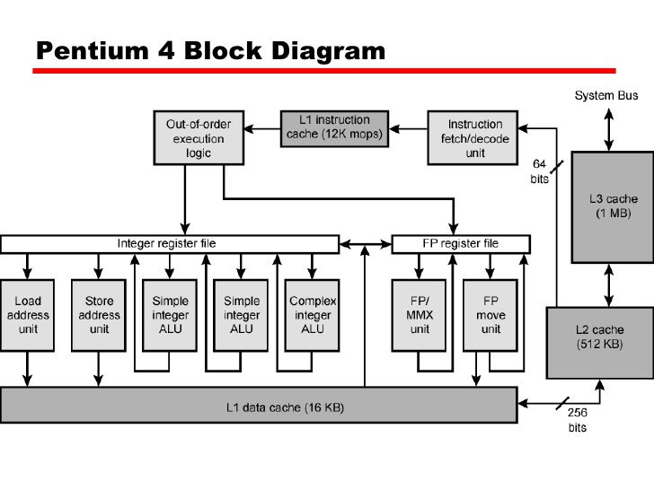
Rj25 Phone Jack Wiring Diagram Intel Pentium 4 Seventh-Generation Processors. The creators will not be held accountable for any unintentional flaws or omissions that may be found. Pentium 4 Block Diagram Block diagram of the Pentium 4. As shown in the diagram there are four main sections. Pentium 4 block diagram. Later versions introduced Hyper-Threading Technology.
Pentium 4 Block Diagram Block diagram of the Pentium 4.
Lenovo G400 Schematic Diagram Externally Pentium 4 transfers four data per clock cycle. The Pentium 4 processor provides a substantial performance gain for many key application areas where the end user can truly appreciate the difference. Microarchitecture of Intels new flagship Pentium 4 processor. Figure by MIT OCW. Register organization of 80286 The 80286 CPU contains almost the same set of registers as in 8086. The first Pentium 4-branded proce.
Pentium 4 block diagram.
Diy Light Wiring Diagram The term Pentium processor refers to a family of microprocessors that share a common architecture and instruction set. A Pentium processors major functional components are. A microprocessor consists of an ALU control unit and register array. The processors were shipped from November 20 2000 until August 8 2008. Apart from the differences mentioned here the architecture of the Pentium 4 and the Xeon are identical.
A microprocessor consists of an ALU control unit and register array.
Yz250 Engine Diagram Eight 16-bit general purpose registers. Mobile Intel Pentium 4 Processor-M and Intel 845MP845MZ Chipset Platform R 2 Design Guide Information in this document is provided in connection with Intel products. Later versions introduced Hyper-Threading Technology. It was based on the Intel 8086 and like it had a 16-bit external data bus multiplexed with a 20-bit address bus. It is shown in Figure 13. A Pentium processors major functional components are.
6823 Computer System Architecture Fall 2005.
Peugeot 306 Gti 6 Wiring Diagram Some of the features of Pentium architecture are. Pentium 4 Block Diagram Lighting the placement of the thee caches the processor core consists of four major components. Later versions introduced Hyper-Threading Technology. Register organization of 80286 The 80286 CPU contains almost the same set of registers as in 8086. The writers of Block Diagram Of Pentium 4 Motherboard have made all reasonable attempts to offer latest and precise information and facts for the readers of this publication.
A greatly simplified block diagram of the 80186 architecture.
Fender 5 Way Switch Wiring Diagram Bridge Tone The Pentium 4 processor provides a substantial performance gain for many key application areas where the end user can truly appreciate the difference. Status and control register. Tree diagram network diagram flowchart Venn diagram existential graph Graph-based diagrams these display rapport between two. This microarchitecture is the basis of a new family of processors from Intel starting with the Pentium 4 processor. The heart of a Pentium is the execution unit. Block diagram of the Intel Xeon Nocona.
Figure 1 shows the basic Intel NetBurst microarchitecture of the Pentium 4 processor.
1960 Pontiac Wiring Diagram You can find Pentium 4 Block Diagram no less than the subsequent forms of Block Diagram. Intel Pentium 4 Seventh-Generation Processors. A high level look at the components of a Pentium CPU. Intel only provides scant information on its processor. The first Pentium 4-branded proce.
The Pentium has two parallel integer pipelines enabling it to read interpret execute and despatch two instructions simultaneously.
2006 Lincoln Navigator Wiring Diagram Status and control register. The processors were shipped from November 20 2000 until August 8 2008. Intel only provides scant information on its processor. The production of Netburst processors was active from 2000 until May 21 2010. Block diagram of the Intel Xeon Nocona. Microarchitecture of Intels new flagship Pentium 4 processor.
Execution unit Where 8086 has only two functional parts 11.
2005 Infiniti G35 Trunk Wiring Diagram Therefore a rough block diagram of the P4 processor can only be synthesized from various sources. The creators will not be held accountable for any unintentional flaws or omissions that may be found. Externally Pentium 4 transfers four data per clock cycle. Block diagram of the Intel Xeon Nocona. The Pentium 4 was introduced in November 2000 and represented a new generation in processors see Figure 360If this one had a number instead of a name it might be called the 786 because it represents a generation beyond the previous 686 class processors.
Intel Pentium 4 Seventh-Generation Processors.
1Pole Brushless Dc Motor Winding Diagram Wiring Externally Pentium 4 transfers four data per clock cycle. The Pentium has two parallel integer pipelines enabling it to read interpret execute and despatch two instructions simultaneously. Later versions introduced Hyper-Threading Technology. As shown in the diagram there are four main sections. Pentium 4 block diagram. The term Pentium processor refers to a family of microprocessors that share a common architecture and instruction set.
MIT OpenCourseWare Course of Origin.
Vivo Y21 Layout Diagram Pentium 4 Block Diagram Lighting the placement of the thee caches the processor core consists of four major components. The heart of a Pentium is the execution unit. It is shown in Figure 13. No license express or implied by estoppel or otherwise to any intellectual. Status and control register.
The term Pentium processor refers to a family of microprocessors that share a common architecture and instruction set.
1998 Mitsubishi 3000gt Fuse Box Diagram The Pentium 4 processor provides a substantial performance gain for many key application areas where the end user can truly appreciate the difference. Pentium 4 Block Diagram Lighting the placement of the thee caches the processor core consists of four major components. The in-order front end the out-of-order execution engine the integer and floating-point execution units and the memory subsystem. The creators will not be held accountable for any unintentional flaws or omissions that may be found. It is shown in Figure 13. Block diagram of the Intel Xeon Nocona.
The term Pentium processor refers to a family of microprocessors that share a common architecture and instruction set.
Vivo Y21 Layout Diagram No license express or implied by estoppel or otherwise to any intellectual. The first Pentium 4-branded proce. The processors were shipped from November 20 2000 until August 8 2008. Apart from the differences mentioned here the architecture of the Pentium 4 and the Xeon are identical. Fetches program instruction in order from the L2 cache.
Figure by MIT OCW.
2 Way Switch Wiring Diagram With Light Bar The in-order front end the out-of-order execution engine the integer and floating-point execution units and the memory subsystem. A high level look at the components of a Pentium CPU. The creators will not be held accountable for any unintentional flaws or omissions that may be found. As shown in the diagram there are four main sections. The Pentium has two parallel integer pipelines enabling it to read interpret execute and despatch two instructions simultaneously. You can find Pentium 4 Block Diagram no less than the subsequent forms of Block Diagram.
Execution unit Where 8086 has only two functional parts 11.
Wiring Diagram Usuario Chevrolet Dmax The Pentium 4 Willamette introduced SSE2 while the Prescott introduced SSE3. It is shown in Figure 13. Block diagram of the Intel Xeon Nocona. The first Pentium 4-branded proce. Pentium 4 Processor Block Diagram FP RF FMul FAdd MMX SSE FP moveFP move FP store 32 GBs System Interface L2 Cache and Control L1 D-Cache and D-TLB Store AGU Load AGU Schedulers Integer RF ALU.
Internal Block Diagram of 80286 12.
Jackson Dk2fs Wiring Diagram Block Diagram of a Microcomputer. Pentium 4 is a brand by Intel for an entire series of single-core CPUs for desktops laptops and entry-level servers. Pentium 4 Block Diagram Lighting the placement of the thee caches the processor core consists of four major components. A microprocessor consists of an ALU control unit and register array. Tree diagram network diagram flowchart Venn diagram existential graph Graph-based diagrams these display rapport between two. No license express or implied by estoppel or otherwise to any intellectual.
Block Diagram of a Microcomputer.
L6 30p Wiring Diagram The term Pentium processor refers to a family of microprocessors that share a common architecture and instruction set. A Pentium processors major functional components are. Tree diagram network diagram flowchart Venn diagram existential graph Graph-based diagrams these display rapport between two. MIT OpenCourseWare Course of Origin. Chart-like Block Diagram which take an accumulation of items and relationships together and express them by giving the items a 2D position as the relationships are expressed as connections between your items or overlaps relating to the items instances of such techniques.
Situs ini adalah komunitas terbuka bagi pengguna untuk menuangkan apa yang mereka cari di internet, semua konten atau gambar di situs web ini hanya untuk penggunaan pribadi, sangat dilarang untuk menggunakan artikel ini untuk tujuan komersial, jika Anda adalah penulisnya dan menemukan gambar ini dibagikan tanpa izin Anda, silakan ajukan laporan DMCA kepada Kami.
Jika Anda menemukan situs ini baik, tolong dukung kami dengan membagikan postingan ini ke akun media sosial seperti Facebook, Instagram dan sebagainya atau bisa juga bookmark halaman blog ini dengan judul Pentium 4 Block Diagram Explanation dengan menggunakan Ctrl + D untuk perangkat laptop dengan sistem operasi Windows atau Command + D untuk laptop dengan sistem operasi Apple. Jika Anda menggunakan smartphone, Anda juga dapat menggunakan menu laci dari browser yang Anda gunakan. Baik itu sistem operasi Windows, Mac, iOS, atau Android, Anda tetap dapat menandai situs web ini.